|
No hay comentarios de productos.
SECTION 2 DIAGRAMS
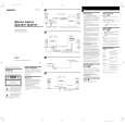
2-1. IC BLOCK DIAGRAM
� IC1, IC2 TEA2025B
+Vs 16
OUT1 15
BOOT1 14
GND 13
GND 12
FEED BACK 11
50
IN1+ 10
GND 9
THERMAL
10K
PROTECT.
START CIRCUIT DECOUPLING
50
5K
10K 50
1
BRIDGE
2
OUT2
3
BOOT2
4
GND
5
GND
6
FEED BACK
7
IN2+
8
SVR
Note on Printed Wiring Board: � X : parts extracted from the component side. � b : Pattern from the side which enables seeing. Note on Schematic Diagram: � All capacitors are in µF unless otherwise noted. pF: µµF 50 WV or less are not indicated except for electrolytics and tantalums. � All resistors are in � and 1/4 W or less unless otherwise specified. � C : panel designation. � U : B+ Line. � Power voltage is dc 9 V and fed with regulated dc power supply from battery terminal. � Voltages and waveforms are dc with respect to ground under no-signal (detuned) conditions. � Voltages are taken with a VOM (Input impedance 10 M�). Voltage variations may be noted due to normal production tolerances. � Signal path. E : AUDIO signal
�3�
|