|
No hay comentarios de productos.
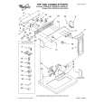
SCHEMATIC DIAGRAM 40PW03B
MODEL :
40PW03G /
CAUTION: The international hazard symbols "*" in the schematic diagram and the parts list designate components which have special characteristics important for safety and should be replaced only with types identical to those in the original circuit or specified in the parts list. The mounting position of replacements is to be identical with originals. Before replacing any of these components, read carefully the PRODUCT SAFETY NOTICE on page 3. Do not degrade the safety of the receiver through improper servicing.
CBSERVATION OF VOLTAGES AND WAVEFORMS 1. Voltages read with VTVM from point shown to chassis ground, line voltages 220 volts, colour bar signal. Voltage reading may vary ±20%. 2. All waveforms are taken using a wide band oscilloscope and a low capacity probe. 3. Waveforms are taken using a standard colour bar signal. 4. Make sure that CONTRAST and COLOUR controls are in mid position and BRIGHTNESS control is almost in maximum position. Set other controls for best picture.
NOTES: 1. D.C. resistance value of a principal transformer is shown in this schematic diagram. These are measured for separated from the circuit. 2. The circuits are subject to change without notice. 3. : Solder links.
EXPRESSION VALUE OF RESISTOR, CAPACITOR and INDUCTOR 1. Resistance is shown in ohm, K=1,000, M=1,000,000 2. Unless other wise noted in schematic, all capacitor values less than 1 are expressed in ?F and the values more than 1 in pF. 3. Unless other wise noted in schematic, all inductor values more than 1 are expressed in ?H, and the values less than 1 in H.
|