|
|
|
Productos
|
|
Información
|
|
Destacado
|
|
|
No hay comentarios de productos.
1
2
3
4
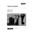
SD-T50W1
3. PCB CONNECTION DIAGRAM
To POWER SUPPLY ASSY J101 E14
NOTE FOR PCB DIAGRAMS:
1. Part numbers in PCB diagrams match those in the schematic diagrams. 2. A comparison between the main parts of PCB and schematic diagrams is shown below.
Symbol in PCB Diagrams Symbol in Schematic Diagrams Part Name
A
To T1 POWER TRANSFORMER
Symbol in PCB Diagrams
Symbol in Schematic Diagrams
Part Name
3-terminal regulator 3. The parts mounted on this PCB include all necessary parts
B BCE B BCE
C
EB
C
E Transistor
for several destination. For further information for respective destinations, be sure to check with the schematic diagram.
C
EB
C
E Transistor with resistor
4. Viewpoint of PCB diagrams
Connector Capacitor
SIDE A
D DGS
G
SD
G
S Field effect transistor
P. C. Board Chip Part
SIDE B
Resistor array
B
3.1 RELAY ASSY
RELAY ASSY
SIDE A
C
(ANP1941�A)
To S2 POWER SWITCH
D
To POWER SUPPLY ASSY CN106 E13
21
1 2 3 4
|
|
 |
> |
|